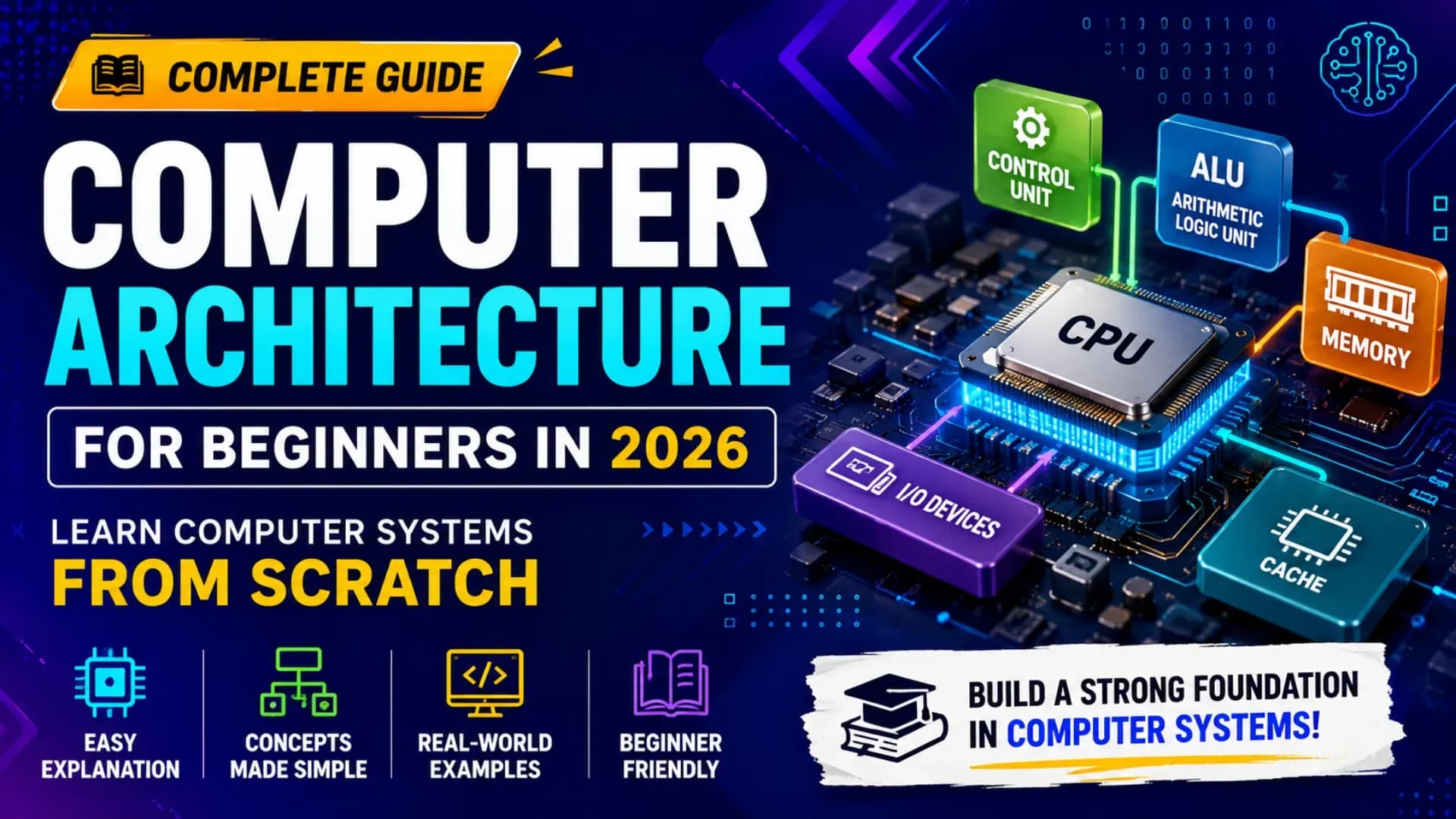
Every program you write runs on hardware. Every line of Python, every database query, every web request eventually resolves to electrical signals moving through silicon. Computer Architecture is the discipline that explains exactly how that happens — how a processor fetches and executes instructions, how memory is organised to balance speed and capacity, how modern CPUs achieve extraordinary performance through parallelism and prediction, and how the entire hardware stack is designed to serve the software running on top of it. This complete Computer Architecture tutorial takes beginners from the foundational Von Neumann model through CPU architecture, instruction set architecture, memory hierarchy, pipelining concepts, and the modern design techniques that make today's processors possible. This computer systems guide 2026 includes diagrams, working examples, and a clear learning path — everything you need to learn computer architecture from scratch and build the computer hardware fundamentals knowledge that underpins all of systems programming, embedded development, and computer science study.
Related Article:
Top BTech Colleges in India 2026
Table of Contents
- Foundations — Von Neumann Architecture and Computer Organisation
- Instruction Set Architecture — The Hardware-Software Interface
- CPU Architecture — Datapath and Control
- Pipelining Concepts — How CPUs Overlap Execution
- Memory Hierarchy — Registers to RAM to Disk
- Modern CPU Architecture — Superscalar, OoO, and Branch Prediction
- I/O and Buses — Connecting the System
- Next Steps — Computer Architecture Learning Path 2026
Foundations — Von Neumann Architecture and Computer Organisation
All modern computers — from a microcontroller in a washing machine to a data centre server — are implementations of the Von Neumann architecture proposed by John von Neumann in 1945. The core idea: store both program instructions and data in the same memory, and build a processor that fetches instructions from memory and executes them sequentially.
# The Von Neumann Architecture — five key components:
#
# ┌─────────────────────────────────────────────────────┐
# │                  MAIN MEMORY (RAM)                   │
# │  Stores both: PROGRAM INSTRUCTIONS + DATA            │
# │  Address 0x0000: instruction (MOV R1, 5)             │
# │  Address 0x0004: instruction (ADD R1, R2)            │
# │  Address 0x1000: data        (value = 42)            │
# └─────────────────┬───────────────────────────────────┘
#                   │  Memory Bus (address + data + control)
# ┌─────────────────▼───────────────────────────────────┐
# │          CENTRAL PROCESSING UNIT (CPU)               │
# │                                                      │
# │  ┌─────────────────┐  ┌──────────────────────────┐  │
# │  │ CONTROL UNIT    │  │ ARITHMETIC LOGIC UNIT    │  │
# │  │ Decodes instr.  │  │ Performs ADD, SUB, AND,  │  │
# │  │ Sequences ops   │  │ OR, XOR, compare, shift  │  │
# │  └─────────────────┘  └──────────────────────────┘  │
# │  ┌─────────────────────────────────────────────────┐ │
# │  │  REGISTERS — tiny ultra-fast on-chip storage    │ │
# │  │  PC (Program Counter): address of next instr.   │ │
# │  │  IR (Instruction Register): current instruction │ │
# │  │  MAR (Memory Address Register): memory address  │ │
# │  │  MDR (Memory Data Register): data to/from mem   │ │
# │  │  R0–R15: general-purpose registers              │ │
# │  └─────────────────────────────────────────────────┘ │
# └─────────────────────────────────────────────────────┘
#                   │
# ┌─────────────────▼───────────┐  ┌─────────────────────┐
# │  INPUT DEVICES               │  │ OUTPUT DEVICES       │
# │  Keyboard, mouse, NIC, disk  │  │ Display, printer, NIC│
# └──────────────────────────────┘  └─────────────────────┘
# The Fetch-Decode-Execute Cycle — how the CPU runs programs:
#
# FETCH: PC → MAR → memory read → instruction → IR; PC = PC + 4
# DECODE: Control Unit interprets IR: what operation? what operands?
# EXECUTE: ALU performs operation; result written to register or memory
# REPEAT
#
# Example trace for: ADD R3, R1, R2 (R3 = R1 + R2)
#
# Step 1 FETCH: PC = 0x0008; Memory[0x0008] → IR = 0x00611820
# Step 2 DECODE: Opcode=ADD, src1=R1, src2=R2, dest=R3
# Step 3 EXECUTE: ALU: R1(5) + R2(7) = 12; write 12 → R3
# Step 4: PC = 0x000C (next instruction)
#
# At 3 GHz: one cycle = 0.33 nanoseconds
# Modern CPUs complete ~4 instructions per cycle (IPC)
# → ~12 billion instructions per second per coreThe Von Neumann Bottleneck: Because instructions and data share the same memory and bus, the CPU spends significant time waiting for memory. The entire discipline of computer organisation — caches, pipelines, out-of-order execution — is largely a set of engineering solutions to this fundamental bottleneck.
Instruction Set Architecture — The Hardware-Software Interface
The Instruction Set Architecture (ISA) is the contract between hardware and software — the complete specification of what instructions a processor can execute, how they are encoded as binary, and what registers and memory model the software can assume. The ISA is what a compiler targets when it converts high-level code to machine code.
# ISA defines:
#   1. Instruction types and operations
#   2. Instruction encoding (how bits represent instructions)
#   3. Register set (how many, what size)
#   4. Addressing modes (how operands are specified)
#   5. Memory model (byte-addressable? endianness?)
#   6. Exception and interrupt model
#
# Major ISA families in 2026:
#   x86-64 (Intel/AMD)  — dominant in desktops, servers, laptops
#   ARM64 (AArch64)     — dominant in smartphones, Apple Silicon, IoT
#   RISC-V              — open-source ISA, rapidly growing in academia
#   MIPS                — historically used in embedded, now largely ARM
#   PowerPC             — IBM servers, game consoles (Xbox 360, PS3)
# RISC vs CISC — the two design philosophies:
#
# CISC (Complex Instruction Set Computer):
# Many complex instructions; variable-length encoding
# Instructions can operate directly on memory
# Example: x86 MOVSB copies a byte from [ESI] to [EDI] in one instruction
# Smaller code size; complex decoder hardware
# x86 has ~1,500+ instructions in its full ISA
#
# RISC (Reduced Instruction Set Computer):
# Few simple instructions; fixed-length encoding (4 bytes each)
# Load/Store architecture: ALU ops only on registers
# Memory access only through explicit LOAD and STORE instructions
# Simpler decoder; easier to pipeline (key advantage)
# ARM64 has ~200 base instructions
#
# Modern reality: x86 CPUs decode CISC instructions into
# RISC-like micro-operations (µops) internally —
# so the CISC/RISC distinction is now largely at the ISA level,
# not the microarchitecture level# RISC-V instruction format (fixed 32-bit encoding):
#
# R-type (register operations): ADD, SUB, AND, OR, XOR, SLT
# ┌──────┬─────┬─────┬─────┬──────┬────────┐
# │funct7│ rs2 │ rs1 │funct│ rd │ opcode │
# │ 7bit │ 5b │ 5b │ 3b │ 5b │ 7b │
# └──────┴─────┴─────┴─────┴──────┴────────┘
# rd = rs1 OP rs2
#
# I-type (immediate / load): ADDI, LW, JALR
# ┌────────────┬─────┬─────┬──────┬────────┐
# │ imm[11:0] │ rs1 │funct│ rd │ opcode │
# │ 12 bits │ 5b │ 3b │ 5b │ 7b │
# └────────────┴─────┴─────┴──────┴────────┘
# rd = rs1 + sign_extend(imm)
# LW rd, offset(rs1): load word from memory[rs1 + offset] → rd
#
# S-type (store): SW, SB, SH
# ┌──────────┬─────┬─────┬─────┬──────────┬────────┐
# │imm[11:5] │ rs2 │ rs1 │funct│ imm[4:0] │ opcode │
# └──────────┴─────┴─────┴─────┴──────────┴────────┘
# memory[rs1 + offset] = rs2
#
# B-type (branch): BEQ, BNE, BLT, BGE
# Encodes PC-relative offset for conditional jumps# Addressing modes — how operands are specified:
#
# Immediate: ADD R1, R1, #5 → R1 = R1 + 5 (5 is in the instruction)
# Register: ADD R3, R1, R2 → R3 = R1 + R2
# Direct: MOV R1, [0x1000] → R1 = Memory[0x1000]
# Indirect: MOV R1, [R2] → R1 = Memory[R2]
# Base+Offset: LW R1, 8(R2) → R1 = Memory[R2 + 8] ← most common in RISC
# PC-relative: BEQ R1, R2, +12 → if R1==R2: PC = PC + 12
#
# Base+Offset is how arrays, structs, and stack frames are accessed
# Example: stack frame access in a function
# LW R3, 0(sp) # load return address
# LW R4, 4(sp) # load saved register
# LW R5, 8(sp) # load local variableAlso Read:
Top MTech Colleges in India 2026
CPU Architecture — Datapath and Control
The CPU architecture is the implementation of the ISA in hardware — the actual circuits that fetch, decode, and execute instructions. Understanding the datapath and control unit is the core of computer organisation study and the bridge between logical operation and physical implementation.
# Single-cycle CPU datapath — one instruction per clock cycle:
#
# FETCH stage:
#   PC → Instruction Memory → 32-bit instruction
#   PC + 4 → PC (or PC + branch_offset if branch taken)
#
# DECODE stage:
#   instruction[6:0]   → opcode   → Control Unit generates control signals
#   instruction[11:7]  → rd       → destination register
#   instruction[19:15] → rs1      → Register File read port 1
#   instruction[24:20] → rs2      → Register File read port 2
#   instruction[31:20] → imm12    → Sign Extender → 32-bit immediate
#
# EXECUTE stage:
#   ALU receives: rs1_data, (rs2_data OR immediate) per ALUSrc control
#   ALU operation: ADD/SUB/AND/OR/XOR/SLT per ALUOp control
#   ALU outputs: result, Zero flag (used by branch logic)
#
# MEMORY stage (for LOAD/STORE):
#   Data Memory: ALU result → address
#   STORE: rs2_data → Data Memory[address]
#   LOAD:  Data Memory[address] → read_data
#
# WRITEBACK stage:
#   MemToReg mux: select (ALU result) or (memory read_data)
#   Write result → Register File[rd]
# ALU — the computational core of CPU architecture:
#
# Inputs: A (32-bit), B (32-bit), ALUControl (4-bit)
# Outputs: Result (32-bit), Zero (1-bit), Overflow (1-bit), Carry (1-bit)
#
# ALUControl → Operation:
# 0000 → AND result = A & B
# 0001 → OR result = A | B
# 0010 → ADD result = A + B
# 0110 → SUB result = A - B (uses adder with B inverted + Cin=1)
# 0111 → SLT result = (A < B) ? 1 : 0
# 1100 → NOR result = ~(A | B)
# 1000 → XOR result = A ^ B
# 1001 → SHL result = A << B[4:0]
# 1010 → SHR result = A >> B[4:0] (logical)
#
# Zero flag: result == 0 → Zero = 1
# Used by BEQ: if Zero=1 after SUB(R1,R2), branch is taken
def alu(A, B, op):
"""Simple 32-bit ALU simulation."""
mask = 0xFFFFFFFF
ops = {
'AND': A & B, 'OR': A | B, 'XOR': A ^ B,
'ADD': (A + B) & mask, 'SUB': (A - B) & mask,
'SLT': 1 if A < B else 0,
'SHL': (A << (B & 31)) & mask,
'SHR': A >> (B & 31),
}
result = ops[op]
zero = 1 if result == 0 else 0
return result, zero
# BEQ instruction: branch if R1 == R2
result, zero = alu(42, 42, 'SUB')
print(f"SUB(42,42) = {result}, Zero = {zero}") # 0, 1 → branch taken
result, zero = alu(42, 43, 'SUB')
print(f"SUB(42,43) = {result}, Zero = {zero}") # non-zero, 0 → no branch# Control Unit — generates control signals from opcode:
#
# Opcode (7-bit RISC-V) → Control Signals:
#
# Instruction opcode RegWrite MemRead MemWrite MemToReg ALUSrc Branch
# ─────────────────────────────────────────────────────────────────────────
# R-type (ADD) 0110011 1 0 0 0 0 0
# I-type (LW) 0000011 1 1 0 1 1 0
# S-type (SW) 0100011 0 0 1 X 1 0
# B-type (BEQ) 1100011 0 0 0 X 0 1
# U-type (LUI) 0110111 1 0 0 0 1 0
#
# RegWrite=1: write result to rd in register file
# MemRead=1: read from data memory
# MemWrite=1: write to data memory
# MemToReg=1: writeback from memory (not ALU result)
# ALUSrc=1: second ALU input = immediate (not rs2)
# Branch=1: enable branch logic (check Zero flag)Pipelining Concepts — How CPUs Overlap Execution
Pipelining concepts are the most important single performance technique in CPU architecture. A pipeline divides the fetch-decode-execute cycle into stages and processes multiple instructions simultaneously — like an assembly line where each station works on a different car at the same time.
# Without pipelining (single-cycle): one instruction at a time
#
# Time:  1  2  3  4  5  6  7  8  9  10  11  12
# I1:    F  D  E  M  W
# I2:                F  D   E   M   W
# I3:                              F  D   E   M  W
# 3 instructions take 15 cycles (5 stages each)
#
# With 5-stage pipeline: overlap stages
#
# Time:  1   2   3   4   5   6   7
# I1:    F   D   E   M   W
# I2:        F   D   E   M   W
# I3:            F   D   E   M   W
# I4:                F   D   E   M   W
# I5:                    F   D   E   M   W
#
# 5 instructions take 9 cycles (not 25)
# Throughput: 1 instruction completes per cycle (in steady state)
# Speedup approaches N for an N-stage pipeline
#
# Stages:  F=Fetch  D=Decode  E=Execute  M=Memory  W=Writeback
# Pipeline Hazards — the three problems that disrupt pipelines:
#
# 1. STRUCTURAL HAZARD: two instructions need the same hardware simultaneously
# Solution: duplicate resources (separate instruction and data caches)
#
# 2. DATA HAZARD: instruction needs result not yet computed by earlier instruction
# Example (RAW — Read After Write):
# ADD R3, R1, R2 ← writes R3 at end of cycle 5
# SUB R4, R3, R5 ← reads R3 at beginning of cycle 4 → STALE VALUE!
#
# Solution A: Stall (insert NOPs — "bubble" in pipeline)
# Time: 1 2 3 4 5 6 7 8 9
# ADD: F D E M W
# NOP: F D E M W
# NOP: F D E M W
# SUB: F D E M W ← now gets correct R3
# Cost: 2 wasted cycles per RAW hazard
#
# Solution B: Forwarding (bypass) — route ALU result directly to next stage
# After ADD's Execute stage: forward R3 directly to SUB's Execute input
# No stall needed for most RAW hazards — hardware detects and routes
# Modern CPUs implement forwarding extensively
#
# 3. CONTROL HAZARD: branch outcome not known until Execute stage
# Pipeline already fetched 2 instructions that may be wrong!
# Solution A: Flush — discard wrong instructions (2 cycle penalty)
# Solution B: Branch prediction (see Modern CPU section)# Pipeline simulation in Python:
def simulate_pipeline(instructions, hazard_stalls=0):
"""
Simulate a 5-stage pipeline.
hazard_stalls: stall cycles inserted per instruction pair
Returns total cycles to complete all instructions.
"""
stages = ['F', 'D', 'E', 'M', 'W']
n = len(instructions)
pipeline_stages = 5
# Without pipeline: n * stages cycles
single_cycle_time = n * pipeline_stages
# With pipeline: pipeline_stages + (n-1) + stalls
pipeline_time = pipeline_stages + (n - 1) + hazard_stalls
speedup = single_cycle_time / pipeline_time
print(f"Instructions: {n}")
print(f"Single-cycle: {single_cycle_time} cycles")
print(f"Pipelined: {pipeline_time} cycles")
print(f"Stall cycles: {hazard_stalls}")
print(f"Speedup: {speedup:.2f}x")
return pipeline_time
# 10 instructions, 3 data hazard stalls (forwarding handles most)
simulate_pipeline(["ADD","LW","SUB","AND","OR","BEQ","LW","ADD","SW","JAL"], 3)
# Single-cycle: 50 cycles | Pipelined: 18 cycles | Speedup: ~2.8xMemory Hierarchy — Registers to RAM to Disk
The memory hierarchy is one of the most practically important concepts in computer hardware fundamentals. The central problem: fast memory is expensive and small; large memory is slow. The solution: build a hierarchy of storage levels, each faster but smaller than the next, and exploit the fact that programs tend to access the same data repeatedly (temporal locality) and nearby data (spatial locality).
# Memory hierarchy — speed, size, cost at each level (2026 typical values):
#
# Level        Size          Latency      Bandwidth    Cost/GB
# ──────────────────────────────────────────────────────────────
# Registers    256 bytes     0.3 ns       ~TB/s        —
# L1 Cache     32–64 KB      1 ns         ~1 TB/s      —
# L2 Cache     256 KB–1 MB   4 ns         ~400 GB/s    —
# L3 Cache     8–64 MB       20–40 ns     ~200 GB/s    —
# DRAM (RAM)   8–512 GB      70–100 ns    ~50–100 GB/s $4
# NVMe SSD     500 GB–8 TB   100 µs       ~7 GB/s      $0.10
# HDD          1–20 TB       5–10 ms      ~200 MB/s    $0.02
# ──────────────────────────────────────────────────────────────
# Key insight: DRAM is 100x slower than L1 cache
# A cache miss to RAM costs ~200–300 cycles of CPU time
# A disk access costs ~10 million cycles
# Cache operation — how the memory hierarchy works:
#
# When CPU needs data at address A:
# 1. Check L1 cache: HIT → data in 1 ns; MISS → check L2
# 2. Check L2 cache: HIT → data in 4 ns; MISS → check L3
# 3. Check L3 cache: HIT → data in 20ns; MISS → go to DRAM
# 4. DRAM access: data in 70–100 ns; also load block into all caches
#
# Cache organisation — direct-mapped cache example:
# Cache size: 1 KB = 16 lines × 64-byte blocks
# Memory address (32-bit) split into:
# ┌─────────────────┬────────────┬──────────┐
# │ Tag (20b) │ Index (4b) │ Offset(6b│
# └─────────────────┴────────────┴──────────┘
# Index: selects cache line (0–15)
# Offset: selects byte within 64-byte block
# Tag: stored alongside cache line; compared to verify HIT
#
# Cache policies:
# Write-through: write to cache AND memory simultaneously
# Write-back: write to cache only; write to memory on eviction
# LRU eviction: evict least recently used line on cache full# Locality — why caches work so well:
#
# Temporal locality: if you access data[5] now, you'll likely access
# it again soon → keep it in cache
#
# Spatial locality: if you access data[5], you'll likely access
# data[6], data[7], data[8] soon → load the whole 64-byte block
#
# Locality in code — cache-friendly vs cache-unfriendly:
import time
N = 1024
matrix = [[1] * N for _ in range(N)]
# Cache-FRIENDLY (row-major traversal — sequential memory access):
t0 = time.perf_counter()
total = sum(matrix[i][j] for i in range(N) for j in range(N))
t1 = time.perf_counter()
print(f"Row-major (cache-friendly): {t1-t0:.4f}s")
# Cache-UNFRIENDLY (column-major — jumps 1024 elements = 4KB gap):
t0 = time.perf_counter()
total = sum(matrix[i][j] for j in range(N) for i in range(N))
t1 = time.perf_counter()
print(f"Column-major (cache-unfriendly): {t1-t0:.4f}s")
# Row-major is typically 3–10x faster due to cache behaviourModern CPU Architecture — Superscalar, Out-of-Order, and Branch Prediction
The simple 5-stage pipeline described above is a teaching model. Modern CPU architecture adds three further techniques — superscalar execution, out-of-order execution, and branch prediction — that together explain why a 2026 CPU can sustain 4+ instructions per cycle.
# 1. SUPERSCALAR EXECUTION — multiple execution units:
#
# Simple pipeline: 1 instruction per cycle (IPC = 1)
# Superscalar: multiple pipelines; dispatch multiple instructions/cycle
#
# Modern Intel/AMD cores have:
#   4–6 integer execution units (ALUs)
#   2–4 FPU / vector execution units (for floating-point and SIMD)
#   2 load units + 2 store units (memory execution)
#   Total: dispatches up to 6 µops per cycle
#
# Apple M4 cores dispatch up to 9 instructions per cycle
# Intel Core Ultra dispatches up to 6 µops per cycle
#
# 2. OUT-OF-ORDER EXECUTION (OoO) — execute in dependency order:
#
# Problem: instruction I3 depends on I1 (data hazard)
#          but I2 is independent of I1
#
# In-order pipeline:  I1 → STALL → STALL → I2 → I3  (wasted cycles)
# Out-of-order:       I1 and I2 execute in parallel
#                     I3 executes after I1 completes
#                     Results committed in original program order (ROB)
#
# OoO engine components:
#   Instruction Queue: buffers decoded instructions
#   Dispatch/Issue: examines ready instructions; issues to execution units
#   Reservation Stations: hold waiting instructions until operands ready
#   Reorder Buffer (ROB): tracks in-flight instructions; commits in order
#   Register Renaming: eliminates false dependencies (WAR, WAW hazards)
# 3. BRANCH PREDICTION — guessing the outcome of conditional branches:
#
# Problem: BEQ R1, R2, +48 — taken or not taken?
# Pipeline fetches next instructions before BEQ resolves
# If prediction wrong: flush pipeline (15–20 cycle penalty)
#
# Branch predictor types:
#
# Static: always predict not-taken (wrong ~50% for loops)
#
# 2-bit saturating counter (simple dynamic predictor):
# State: Strongly Not Taken (00) → Weakly NT (01) → Weakly Taken (10) → Strongly Taken (11)
# Prediction: state >= 10 → predict Taken
# Update: if branch taken → increment; if not taken → decrement
# For a loop executing 100 times: mispredicts only at entry and exit
# Accuracy: ~85–90% on typical workloads
#
# TAGE predictor (modern, used in Intel/AMD cores):
# Multiple tables indexed by different lengths of branch history
# Uses longest matching history for prediction
# Accuracy: ~95–97% on SPECint benchmarks
#
# NEURAL branch predictor (Intel 12th gen+, AMD Zen 5):
# Perceptron-based; learns complex history patterns
# Accuracy: ~98%+ on many workloads
def two_bit_predictor(branch_history):
"""Simulate a 2-bit saturating counter branch predictor."""
state = 0b10 # start: Weakly Taken
correct, wrong = 0, 0
for taken in branch_history:
prediction = state >= 0b10 # predict Taken if state >= 2
if prediction == taken:
correct += 1
else:
wrong += 1
# Update state
if taken and state < 0b11: state += 1
elif not taken and state > 0b00: state -= 1
accuracy = correct / len(branch_history) * 100
print(f"Correct: {correct} | Wrong: {wrong} | Accuracy: {accuracy:.1f}%")
# Loop that runs 10 times then exits (taken 10x, not taken 1x)
loop = [True] * 10 + [False]
two_bit_predictor(loop) # Should be ~91% accurateCHECK OUT:
Top Colleges in Ranchi 2026
I/O and Buses — Connecting the System
The CPU and memory do not operate in isolation — they are connected to I/O devices, storage, and other processors through a system of buses and interconnects. Understanding the bus hierarchy is the final piece of computer organisation and computer hardware fundamentals.
# Modern computer system bus hierarchy (2026):
#
# ┌──────────────────────────────────────────────────┐
# │  CPU DIE                                          │
# │  ┌──────────┐  ┌──────────┐  ┌──────────────┐   │
# │  │ Core 0   │  │ Core 1   │  │   ...Core N  │   │
# │  │ L1+L2    │  │ L1+L2    │  │              │   │
# │  └────┬─────┘  └────┬─────┘  └──────┬───────┘   │
# │       └─────────────┴────────────────┘            │
# │              Ring Bus / Mesh Network               │
# │       ┌─────────────────────────────────┐          │
# │       │        L3 Cache (shared)         │          │
# │       └──────────────┬──────────────────┘          │
# │                      │                             │
# │       ┌──────────────▼──────────────────┐          │
# │       │  Memory Controller (IMC)         │          │
# │       └──────────────┬──────────────────┘          │
# └──────────────────────┼──────────────────────────────┘
#                        │
#          DDR5 DRAM     │ DRAM Bus (64-bit, ~6400 MT/s)
# ┌────────────────────────────────────────────────────┐
# │  PCIe 5.0 Bus (16 lanes = 128 GB/s bidirectional)  │
# │  ├── GPU (discrete graphics / compute)              │
# │  ├── NVMe SSD (PCIe 4.0/5.0 — up to 14 GB/s)      │
# │  └── Network Card (100 GbE — 12.5 GB/s)            │
# ├────────────────────────────────────────────────────┤
# │  USB 4 / Thunderbolt 4 (40 Gbps = 5 GB/s)          │
# │  SATA (6 Gbps = 600 MB/s — for older HDDs/SSDs)    │
# └────────────────────────────────────────────────────┘
# Bus performance — bandwidth and latency matter differently:
#
# BANDWIDTH: how much data per second (GB/s, Gbps)
# Critical for: GPU, NVMe SSD, network — streaming large data
# DDR5-6400: 51 GB/s per channel, 102 GB/s dual-channel
#
# LATENCY: time from request to first data byte
# Critical for: CPU caches, DRAM random access, storage IOPS
# PCIe has ~1 µs overhead even at high bandwidth
# This is why GPU memory access from CPU is expensive
#
# IOPS: I/O Operations Per Second (for random access storage)
# NVMe SSD: ~1 million IOPS (4KB random reads)
# HDD: ~100–200 IOPS (seek time dominated)
#
# Why CPU-GPU data transfer is expensive:
# GPU has its own GDDR6 memory (768 GB/s bandwidth on RTX 5090)
# CPU DRAM → GPU VRAM: PCIe 5.0 x16 = 128 GB/s (6x slower)
# + PCIe latency overhead per transfer
# Solution: unified memory architectures (Apple M-series, AMD APUs)Next Steps — Computer Architecture Learning Path 2026
# Your computer architecture progression after this tutorial:
#
# LEVEL 1 — Foundations (this tutorial):
#   ✓ Von Neumann architecture and fetch-decode-execute
#   ✓ Instruction Set Architecture — RISC vs CISC, RISC-V encoding
#   ✓ CPU architecture — datapath, ALU, control unit
#   ✓ Pipelining concepts — stages, hazards, forwarding
#   ✓ Memory hierarchy — registers through disk; cache operation
#   ✓ Modern CPU — superscalar, OoO, branch prediction
#   ✓ I/O and buses — PCIe, DDR5, NVMe
#
# LEVEL 2 — Intermediate:
#   → Build a RISC-V processor in Verilog/VHDL (HDL simulation)
#     Resources: MIT 6.004, CMU 18-447, UC Berkeley CS152
#   → "Computer Organisation and Design RISC-V Edition"
#     (Patterson and Hennessy — the standard textbook)
#   → Write cache simulators in Python/C
#   → Explore RISC-V assembly with VENUS simulator
#   → Study Tomasulo algorithm for OoO execution
#
# LEVEL 3 — Advanced:
#   → "Computer Architecture: A Quantitative Approach"
#     (Hennessy and Patterson — the graduate textbook)
#   → Study SIMD / vector units (Intel AVX-512, ARM NEON)
#   → GPU architecture (CUDA programming model)
#   → Multiprocessor cache coherence (MESI protocol)
#   → Memory consistency models (TSO, relaxed consistency)
#   → Hardware security (Spectre, Meltdown, microarchitectural attacks)
#
# BEST TOOLS for computer architecture study in 2026:
#   gem5        → full-system architecture simulator (industry standard)
#   VENUS       → RISC-V assembly simulator (browser-based)
#   Logisim     → digital logic circuit simulator
#   Icarus Verilog → open-source Verilog HDL simulator
#   perf        → Linux performance counters (observe real CPU behaviour)
#   valgrind --tool=cachegrind → cache miss analysis on real programs
Best single command to see this computer systems guide 2026 in action: Run valgrind --tool=cachegrind --cache-sim=yes ./your_program on any C program — it reports L1, L2, and L3 cache hit/miss rates, instruction count, and branch misprediction rate. The numbers from this profiler map directly to every concept in this Computer Architecture tutorial. Real hardware, real behaviour, real feedback on whether your code exploits the memory hierarchy well. That is learn computer architecture applied — not abstract.
Explore More
Conclusion
This Computer Architecture tutorial has taken you from the Von Neumann model through every layer of the modern computing stack. The instruction set architecture defines the hardware-software contract — the ISA is what compilers target and what processors implement. CPU architecture — the datapath, ALU, and control unit — is the implementation of that contract in logic gates and registers. Pipelining concepts — the five-stage pipeline, hazards, forwarding, and stalls — explain how modern CPUs achieve throughput far beyond the naive fetch-execute model. The memory hierarchy — from registers through L1/L2/L3 caches to DRAM to SSD — is the engineering solution to the Von Neumann bottleneck, exploiting locality to hide the speed gap between CPU and storage. Modern CPU architecture adds superscalar execution, out-of-order processing, and branch prediction to sustain 4+ instructions per cycle in real workloads.
The computer hardware fundamentals in this computer systems guide 2026 are not academic abstractions — they are the explanation for why cache-friendly code runs 10× faster than cache-unfriendly code, why branch prediction matters for loop performance, why CPU-GPU memory transfer is expensive, and why memory latency is the dominant bottleneck in database and scientific computing workloads. Every software engineer who has worked through this guide to learn computer architecture from scratch will write measurably better software — not because they have memorised architecture diagrams, but because they understand what the hardware is actually doing when their code runs.
This Computer Architecture for beginners guide — the most practically grounded Computer Architecture for beginners resource in this series — is built around a single conviction: computer organization and pipelining concepts are not examination topics, they are explanations for observable behaviour. The instruction set architecture you studied here is the same instruction set architecture your compiler targets today. The pipelining concepts and branch predictor you simulated are the same mechanisms running in the chip under your keyboard. The computer organization principles that connect ALU to register file to cache to DRAM are the same principles that determine whether your matrix multiplication takes 10 milliseconds or 100 milliseconds. This Computer Architecture for beginners foundation, combined with the tools recommended above, gives you the vocabulary to read processor architecture papers, profile code at the hardware level, and make engineering decisions that the majority of software developers — who never studied computer organization — simply cannot make.


